Engineering

Imaging Suite

The Imaging Suite offers a full consultation service to internal, external and industrial clients in the field of materials characterisation for experimental applications at micro and nano scales. It also supports research and teaching in the College of Engineering, Maths and Physical Sciences.

Our services

  • Access to our facilities comes with the associated expert and technical assistance to support routine work on a timed basis or contribute to a significant programme of research and testing.
  • We will work closely with you throughout the process, from the initial project concept to final delivery, to deliver the results to your specification.
  • We are happy to prepare the samples and provide training for customers.
  • In offering these analytical techniques, together with additional expert services, we aim to be a powerful problem solver for the challenges you are seeking to overcome.

To discuss your project, please contact Dr Hong Chang, Imaging Suite Manager.
Imaging Suite equipment

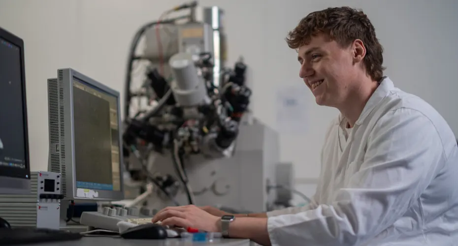
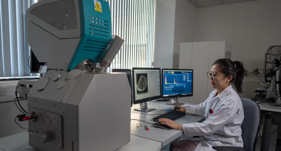
Scanning Electron Microscope (SEM) with Energy Dispersive Spectrometer (EDS)

The TESCAN VEGA3 SEM has both a secondary electron detector and a backscattered electron detector, enabling surface topography imaging at low and high magnifications and/or with atomic number contrast. With a variable pressure mode (VP-SEM), non-conductive samples can be imaged without coating.

In addition, its Oxford Instrument X-MAXN EDS detector enables chemical analysis in the form of point analysis, line analysis or elemental mapping, and sensitive detection of light elements. Applications include metals, ceramics, semiconductors, nanomaterials, composites, polymers and biological materials.

Focused Ion Beam (FIB)

The xT Nova Nanolab 600 FIB is a dual beam unit that combines an electron beam and a Gillum ion beam. It is capable of low and high resolution scanning electron microscopy, scanning ion microscopy, as well as ion beam and electron beam lithography.

It is a versatile tool enabling both sample preparation and imaging in-situ in one unit; the former includes depositing an ultra-thin layer of material onto a sample surface, etching/milling materials and/or patterning, and site specific cross-sectioning of thin film, bulk samples and/or interfaces.

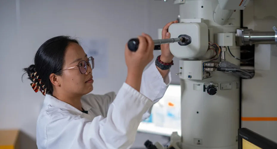
Transmission Electron Microscope (TEM) / Scanning Transmission Electron Microscope (STEM)

The JEOL 2100 TEM is a powerful facility that operates at 200 KV, providing point resolution of 0.25 nm and lattice resolution of 0.14 nm in theory, generating atomic resolution images of nano-materials, thin films, phases, grains, defects and lattice of ultra-thin samples.

It can operate in bright field (BF) and dark field (DF) modes and in both TEM and STEM modes. Fitted with an Oxford Instrument X-MAXN EDS detector, it allows chemical analysis of features as small as a few nanometers. The selected area diffraction (SAED) enables unit cell parameters, orientation and orientation relationships to be identified.

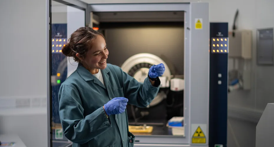
X-Ray Diffractometer (XRD) The Bruker D8 advanced XRD has wide applications in analysing powders, bulk and thin film materials for phase composition (phase ID), quantitative phase analysis, unit lattice parameters, crystal structure, and average crystallite size of nanocrystallines. The combined X-ray-reflectometry (XRR) is useful in thin film thickness, roughness and compositional analysis. With a heating stage capable of running from ambient temperature to 900 ̊C, phase change or chemical reactions in the materials can be captured ‘in-situ’.
Atomic Force Microscope (AFM)

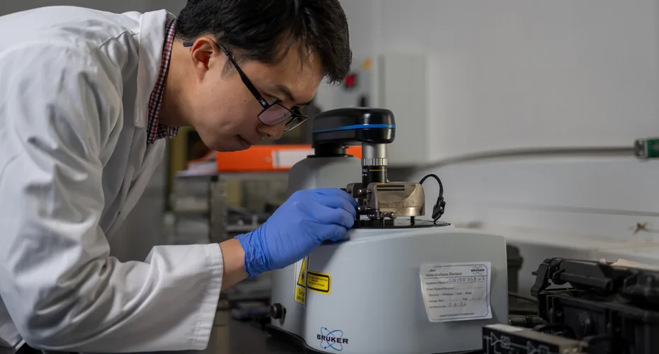
The Bruker Innova AFM is a high resolution scanning probe microscopy facility for true 2D and 3D surface profile, with sub nanometer resolution. It can provide information on surface roughness, magnetic properties, conductivity, and electrostatic properties. Applications include nanomaterials, thin films, bulk materials, composites, polymers, and biological samples.

X-Tek Bench Top Computer Tomography (CT) 160 Xi

The X-Tek CT is a non-destructive X-ray inspection technique capable of producing 2D and 3D maps/structures of materials without damaging the samples. The re-constructed data/structure can be viewed from any 3D angle, sliced in any direction, accurately measured and even animated.

With a resolution of 3 micron in theory, it can accommodate samples from a couple of mm to about 90 mm in diameter. Applications include product quality checking, damage or defect analysis, porosity analysis, composite and laminate materials.